
USB FPGA Module 1.11
Functional description
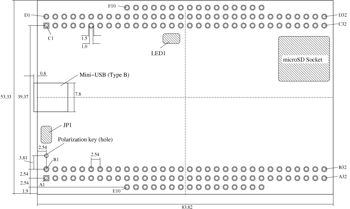
The following drawing shows the measurements and the location of the of the described elements.
Click on the image for a larger version or download the PDF version.
EEPROM address: JP1
Jumper JP1 specifies the I2C address of the EEPROM:
| JP1 | I2C address |
| open | 0xA2 |
| close | 0xAA |
The EZ-USB FX2 Microcontroller searches for the firmware at the address 0xA2 which is the default address (jumper open).
The main purpose of this jumper is to disable the EEPROM boot-load. If, for example, the EEPROM was programmed with a corrupt firmware the Microcontroller can be booted with the internal default firmware by short cutting the two pads of jumper JP1 during powering-on the USB-FPGA-Module.
FPGA state: LED1
LED1 indicates the configuration state of the FPGA as follows:
| LED1 | FPGA |
| on | unconfigured |
| off | configured |
I/O Connector
Two 2x32 pin and two 1x16 pin connectors deliver the I/O signals and are used for the power supply. The drawing shows the position of these connectors.
The I/O connector of the Spartan 6 USB-FPGA-Module 1.11 is mechanical upward compatible to the I/O Connector of the Spartan 3 USB-FPGA-Module 1.2.
The following Pinlist can also be downloaded in Gnumeric or Excel format. These files contains the data for all ZTEX USB-FPGA-Modules and also include a list of connections (several sheets).
| Pinlist | |||||||
| E | A | B | C | D | F | ||
| 1 | 4..35V | 4..35V | USB_5V | USB_5V | 1 | ||
| 2 | GND | GND | 5V (unused) | 5V (unused) | 2 | ||
| 3 | INT4 | T0 | R16~IO_L49N_M1DQ11_1 | 5V (unused) | 3 | ||
| 4 | T1 | T2 | GND | GND | 4 | ||
| 5 | BKPT | GND | INT5# | WAKEUP* | 5 | ||
| 6 | SCL | SDA | 3.3V | 3.3V | 6 | ||
| 7 | 3.3V | 3.3V | 7 | ||||
| 8 | TxD0 | RxD0 | GND | K16~IO_L44N_A2_M1DQ7_1 | 8 | ||
| 9 | B15~IO_L29P_A23_M1A13_1 | B16~IO_L29N_A22_M1A14_1 | PE7/GPIFADR8 | L16~IO_L47N_LDC_M1DQ1_1 | 9 | ||
| 10 | 2.5V | 2.5V | PE6/T2EX | M16~IO_L46N_FOE_B_M1DQ3_1 | N16~IO_L45N_A0_M1LDQSN_1 | 10 | |
| 11 | 1.2V | 1.2V | PE5/INT6 | P16~IO_L48N_M1DQ9_1 | M15~IO_L46P_FCS_B_M1DQ2_1 | 11 | |
| 12 | A14~IO_L65N_SCP2_0 | B14~IO_L65P_SCP3_0 | PE4/RXD1OUT | P15~IO_L48P_HDC_M1DQ8_1 | R15~IO_L49P_M1DQ10_1 | 12 | |
| 13 | A13~IO_L63N_SCP6_0 | C13~IO_L63P_SCP7_0 | GND | PE3/RXD0OUT | T15~IO_L50N_M1UDQSN_1 | L14~IO_L47P_FWE_B_M1DQ0_1 | 13 |
| 14 | C11~IO_L39P_0 | D12~IO_L66N_SCP0_0 | D11~IO_L66P_SCP1_0 | PE2/T2OUT | K15~IO_L44P_A3_M1DQ6_1 | N14~IO_L45P_A1_M1LDQS_1 | 14 |
| 15 | A11~IO_L39N_0 | E11~IO_L64N_SCP4_0 | F10~IO_L64P_SCP5_0 | PE1/T1OUT | R14~IO_L50P_M1UDQS_1 | L13~IO_L53N_VREF_1 | 15 |
| 16 | B10~IO_L35P_GCLK17_0 | 3.3V | 3.3V | PE0/T0OUT | M13~IO_L74P_AWAKE_1 | L12~IO_L53P_1 | 16 |
| 17 | A10~IO_L35N_GCLK16_0 | C10~IO_L37N_GCLK12_0 | E10~IO_L37P_GCLK13_0 | GND | M12~IO_L2P_CMPCLK_2 | R12~IO_L52P_M1DQ14_1 | 17 |
| 18 | F9~IO_L40P_0 | B12~IO_L62P_0 | A12~IO_L62N_VREF_0 | 2.5V | 2.5V | M11~IO_L2N_CMPMOSI_2 | 18 |
| 19 | D9~IO_L40N_0 | A9~IO_L34N_GCLK18_0 | C9~IO_L34P_GCLK19_0 | 1.2V | T12~IO_L52N_M1DQ15_1 | M10~IO_L16N_VREF_2 | 19 |
| 20 | A8~IO_L33N_0 | C8~IO_L38N_VREF_0 | D8~IO_L38P_0 | P8~IO_L30P_GCLK1_D13_2 | R9~IO_L23P_2 | T9~IO_L23N_2 | 20 |
| 21 | B8~IO_L33P_0 | GND | GND | M9~IO_L29P_GCLK3_2 | N9~IO_L14P_D11_2 | P9~IO_L14N_D12_2 | 21 |
| 22 | E8~IO_L36N_GCLK14_0 | VCCO_IO | VCCO_IO | T7~IO_L32N_GCLK28_2 | N8~IO_L29N_GCLK2_2 | T8~IO_L30N_GCLK0_USERCCLK_2 | 22 |
| 23 | E7~IO_L36P_GCLK15_0 | 1.2V | 1.2V | M7~IO_L31N_GCLK30_D15_2 | P7~IO_L31P_GCLK31_D14_2 | R7~IO_L32P_GCLK29_2 | 23 |
| 24 | A7~IO_L6N_0 | C7~IO_L6P_0 | N6~IO_L64N_D9_2 | P6~IO_L47P_2 | T6~IO_L47N_2 | 24 | |
| 25 | E6~IO_L5N_0 | F7~IO_L5P_0 | M6~IO_L64P_D8_2 | P4~IO_L63P_2 | T4~IO_L63N_2 | 25 | |
| 26 | C6~IO_L7N_0 | D6~IO_L7P_0 | GND | GND | 26 | ||
| 27 | A6~IO_L4N_0 | B6~IO_L4P_0 | 27 | ||||
| 28 | C5~IO_L3N_0 | D5~IO_L3P_0 | 1.2V | 1.2V | 28 | ||
| 29 | A5~IO_L2N_0 | B5~IO_L2P_0 | 2.5V | TDI | 29 | ||
| 30 | A4~IO_L1N_VREF_0 | C4~IO_L1P_HSWAPEN_0 | TMS | 30 | |||
| 31 | VCCO_IO | VCCO_IO | TCK | 31 | |||
| 32 | GND | GND | GND | TDO | 32 | ||
| Summary | ||||
| A/B/E | C/D/F | |||
| FPGA-IO | 42 | FPGA-IO | 40 | |
| Serial | 2 | FX2-IO | 8 | |
| I2C | 2 | Wakeup | 1 | |
| Timer | 3 | JTAG | 4 | |
| Interrupt | 1 | Interrupt | 1 | |
| Breakpoint | 1 | USB 5V | 2 | |
| GND | 8 | GND | 7 | |
| 3.3V | 4 | 3.3V | 2 | |
| 1.2V | 4 | 1.2V | 3 | |
| 2.5V | 2 | 2.5V | 3 | |
| VCCO_IO | 4 | 5V | 3 | |
| 4..35V | 2 | NC | 6 | |
| NC | 5 | |||
| FPGA-GPIO | 42 | FPGA-GPIO | 40 | |
| SIO (special I/O) | 9 | FX2-GPIO | 8 | |
| Power | 24 | SIO (special I/O) | 6 | |
| NC | 5 | Power | 20 | |
| Sum | 80 | NC | 6 | |
| Sum | 80 | |||
References
- Product Homepage
- Eagle Library of the I/O connector
- Pinlist and the List of Connections in Gnumeric and Excel format